

The progress made in grid driver IC enables switching power supply to achieve a new power density level
Like many electronic fields, progress continues to occur. At present, in 3.3 kW switching power supply (SMPS), the product efficiency is as high as 98%, with 1U structure size and power density up to 100 W/in ³。 The reason why this can be achieved is that we have wisely selected the super-junction (SJ) power MOSFET (such as CoolMOS) in the totem pole PFC level ™), Silicon carbide (SiC) MOSFET (e.g. CoolSiC ™), In addition, gallium nitride (GaN) power switches (such as CoolGaN ™) For 400V LLC applications. PFC and LLC digital controllers are essential, just as the use of planar magnetic devices and advanced gate driver ICs (such as EiceDRIVER ™) It plays an important role in achieving high performance.Main market trends
When grounding loop isolation must be conducted between two (or more) parts of the system, electrical isolation shall be adopted. The main reasons for adopting electrical isolation are:
Avoid grounding deviation (caused by the normal operation of the power switch) affecting the normal operation of the system.
Prevent surges or pulses from damaging the integrity of the system.
Protect people from harmful electric shock.
VDE 0884-11 is the first industry standard for any electrically isolated semiconductor product (i.e., optical isolation, magnetic isolation or capacitive isolation). It not only considers the barrier characteristics at zero time (i.e., when the manufacturer tests the product). VDE 0884-11 also requires a service life of 20 years. For this reason, the gate driver IC is subject to the time-related dielectric breakdown (TDDB) life test tBD (breakdown time), the upper limit of which is 37.5 years (see Table 1).
However, well-known device-level isolation standards (such as UL 1577, IEC 60747-5-5 or VDE 0884-10, which expire at the same time) have no requirements for product service life.
Since VDE 0884-11 is a German standard, this standard has been merged with the international IEC 60747-17 standard, which is similar to a large extent, and the IEC 60747-17 standard was released on September 20, 2020.
The VDE 0884-11 standard contains a statement that cannot be ignored and is very important:
"Safe electrical isolation can only be guaranteed within the scope of safety level. Compliance with safety level shall be ensured through appropriate protection circuit."
This is especially important when people need to prevent electric shock.
Imagine the worst case of the half-bridge: the high-side MOSFET is short-circuited between the gate and the drain, while the low-side MOSFET is on. In this case of electrical overload ("EOS"), we can observe that more than 600 A current flows to the gate driver IC output. Therefore, in order to protect the IC output end of the gate driver, we add a suppression diode (D1) for the gate resistor (R1) (see Figure 1). The suppression diode provides a bypass for the gate driver output and directs the current to the midpoint of the half-bridge. Therefore, as long as we choose the appropriate application design, the isolation function of the gate driver IC from the output end to the input end can remain unchanged.
Figure 1. EOS test device
In addition to maintaining this isolation function, the exposed metal covered by the molding compound is usually invisible, that is, the integrity of the package must be maintained.
EOS test shows that the gate driver IC is embedded with a barrier at the IC input (such as EiceDRIVER of Infineon Technology Co., Ltd ™ 2EDR series), even without suppression diode D1, can meet these two requirements.
Multiple areas of progress
The startup time of UVLO output stage is short
Since the bootstrap power supply of high side gate driver IC is a very cost-effective solution, this solution is very common. Therefore, half-bridge and full-bridge (typical 400 V DC bus voltage) in high-voltage LLC, or hard-switched full-bridge on the primary side of low-voltage DC-DC converter (for example, 48 V to 12 V) are usually equipped with bootstrap circuit.
The gate driver IC UVLO has a short start-up time, which provides advantages for bootstrap design in many ways:
Fast normal system startup.
The LLC startup time after undervoltage protection is short, for example, more than 200 ms, which is usually equivalent to 10 power cycles.
After the system-level protection is activated, the LLC startup time at the time of restart release is shorter.
During the boost of bootstrap circuit, the main power transformer will not be saturated due to the asymmetry of high side and low side PWM operation.
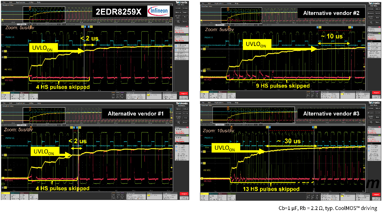
When using a dual-channel electrically isolated gate driver IC with a typical UVLO startup time of 2 µ s on the bootstrap high side, only four high side pulses will be skipped before the half-bridge can start working (provided that the rise of the high side VDD is considered as a typical value). Similar gate driver ICs, whose UVLO start time is 10 µ s or longer, usually skip 10 or more high-side pulses. This greatly extended the start time of half-bridge work (Figure 2).
Appropriate UVLO shutdown time
At the same time, if it only drops below the UVLOoff threshold intermittently, the switch stage should not be turned off.
Practical experience shows that a turn-off delay of 500 ns is a good choice, which can avoid unexpected turn-off of output stage caused by noise or ringing on VDD (for example, caused by load jump).
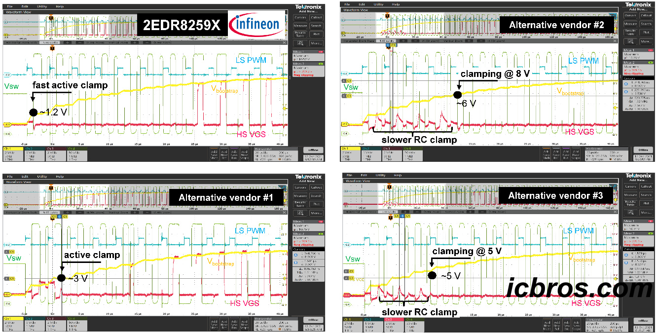
Active output clamping
The purpose of output clamping is to ensure the safe shutdown of the output stage while the grid driver power supply is still below the UVLOon threshold. This reduces the straight-through risk in the process of half-bridge bootstrap.
When the power supply voltage is higher than the UVLOon threshold, the gate driver IC is expected to transmit the control input to the output stage, that is, the output end is no longer clamped, but follows the input signal.
In the bootstrap half-bridge stage, when the low side is switched to boost capacitor charging, the capacitive voltage divider composed of CGD and CGS of the high side switch will cause the VGS to exceed its conduction threshold. The purpose of gate driver IC output clamping is to prevent VGS from exceeding this conduction threshold and effectively short-circuit it. If the output clamping does not occur, the high side switch and the low side switch are connected at the same time, which will form a half-bridge straight-through.
The advanced gate driver IC is equipped with an output clamping circuit, which can be activated at a VDD level as low as 1.2 V, which is very suitable for the "textbook" start of the high side switch (see Figure 3).
In contrast, if the gate driver IC has a built-in slow RC clamping circuit, a certain degree of straight-through will occur during the startup of the half-bridge until the final VDD value is high enough to activate the output clamping circuit. This is not ideal because it will cause electrical overload of switching devices.
Pass-through protection with configurable dead time
The purpose of introducing dead time in the half-bridge is to attenuate the switch tail current after the switch is turned off and before the other side of the half-bridge is turned on. Otherwise, a pass-through event may occur. Super junction power MOSFET (such as CoolMOS of Infineon Technology Co., Ltd ™ ) The typical decay time is within 300 ns.
In a normal working system, the software running in the controller IC meets this dead time. In this way, the controller IC can manage the effective duty cycle of the switch level. When determining the dead-time of software control, the real-time performance of controller IC hardware, operating system and application software all play a role. Therefore, the effective deadband time based on software is usually not less than 300 ns. But in most cases, the dead time is much longer.
In order to prevent the failure of the software-based dead-time control, the pass-through control and dead-time control built in the gate driver IC can be used as the second-level security mechanism to prevent pass-through events.
Modern dual-channel isolated gate driver IC realizes configurable dead time setting through external resistance. The dead time varies from 10 ns to 1000 ns, with large selection space. Therefore, this gate driver IC is very suitable for various power switching technologies, including gallium nitride (GaN) power switches. The dead time accuracy can reach+/- 15%. In fact, this is usually much more accurate than the actual control of the IC based dead-time control.
Packaging innovation
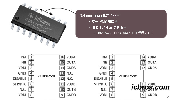
The dual-channel electrically isolated gate driver IC is packaged with 150 mil and 300 mil DSO, usually in a 14-pin configuration. At the gate driver IC level, the difference between the traditional 16-pin configuration and the increasingly popular 14-pin configuration is that the previous "empty" pin at the output end actually no longer exists (Figure 4).
This enables additional PCB top-level wiring. Alternatively, since the resulting creepage distance between channels has increased to 3.4 mm (refer to IEC 60664-1, Class I pollution), the functional isolation voltage between channels up to 1025 VRMS can be achieved.
The package size of the electrically isolated gate driver IC is very important. Designers can now choose a pinless 4x4 mm2 package. Compared with the default 5x5 mm2 package size, the 4x4 mm2 gate driver IC saves 36% of PCB area. The input/output isolation rating is equivalent to VISO=2250 VRMS (UL 1577).
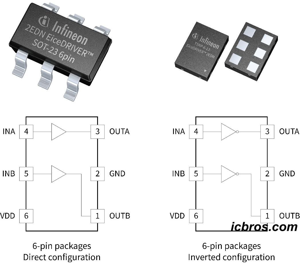
Although most modern dual-channel low-side gate driver ICs have two inputs, these inputs are usually connected to fixed potential, which means that the inputs are not actually used. So, what is the reason for the existence of this input, especially when you want to achieve high power density?
The dual-channel low-side gate driver IC adopts a 6-pin package (if there is a lead SOT-23, or even a lead-less subminiature 1.1x1.5 mm2 6-pin package such as TSNP), which is a very practical and cost-effective solution (Figure 5). In this way, all the advantages of gate driver IC will be reflected, such as digital on/off characteristics, defined UVLO, 5 A strong output stage, and single-digit ns propagation delay accuracy. At the same time, the footprint of PCB is minimized and the flexibility of PCB layout is improved.
conclusion
The gate driver IC integrates electrical isolation, which has developed from a product feature that is certified to be effective only in the zero-hour state to a product feature that specifies a product service life of 20 years. With proper application design, the isolation function and package integrity will not be affected even under severe electrical overload.
Shortening the UVLO startup time accelerates the system startup speed and also avoids the saturation of the main power transformer. Proper UVLO turn-off time can prevent thermal overload of switching devices, and also help to ensure working stability in case of VDD noise or ringing.
Although the grid driver power supply is still lower than the UVLOon threshold, the active output clamp provides a low impedance grounding path for the grid driver IC output. This most general method can avoid half-bridge breakdown event during bootstrap startup.
The gate driver IC hardware has built-in configurable breakdown protection and dead time control, which are important secondary safety mechanisms. Packaging innovation removes unused pins (formerly known as "empty" pins), and the packaging size is also getting smaller and smaller.
ICBROS TECHNOLOGY LIMITED is a worldwide professional electronic components distributor.
【Our hot chip models today:】(In Stock)
Email:service@icbros.com
HK Tel:+852 44058386
Whatsapp:+852 44058386
Skype:jammy@icbros.com
Web:https://www.icbros.com
==============
ADG509FBN SOP16 ADI
ADG509FBRW SOP16 ADI
ADG513BRZ SOP16 ADI
ADM1181AARWZ SOP16 ADI
ADM232AR SOP16 ADI
ADM2483BRW SOP16 ADI
ADM691AARNZ SOP16 ADI
ADM800MARNZ SOP16 ADI
ADUM1301BRW SOP16 ADI
ADUM1401B SOP16 ADI
OP00HS SOP16 ADI
OP413ESZ SOP16 ADI
OP413GS SOP16 ADI
OP420ES SOP16 ADI
OP420ESZ SOP16 ADI
OP420FSZ SOP16 ADI
OP420HS SOP16 ADI
OP420HSZ SOP16 ADI
OP421FSZ SOP16 ADI
OP421G SOP16 ADI
OP421GSZ SOP16 ADI
OP467G SOP16 ADI
OP470ES SOP16 ADI
OP470FS SOP16 ADI
OP470G SOP16 ADI
OP471G SOP16 ADI
OP471GSZ SOP16 ADI
OP490G SOP16 ADI
OP493ES SOP16 ADI
OP493GS SOP16 ADI
OP495GS SOP16 ADI
OP496HS SOP16 ADI
OP497ES SOP16 ADI
OP497ESZ SOP16 ADI
AD694AR SOP-16 ADI
AD694BR SOP-16 ADI
ADG466BRZ SOP18 ADI
AD7392ARZ SOP20 ADI
ADC08061CIWMX SOP20 ADI
DAC8800 SOP20 ADI
AD5204BRU10 SOP24 ADI
AD7237ABR SOP24 ADI
AD7710AR SOP24 ADI
AD7731BR SOP24 ADI
AD7876AR SOP24 ADI
AD7880AR SOP24 ADI
AD7880CR SOP24 ADI
AD7892AR-1 SOP24 ADI
DAC8428F SOP24 ADI
ADC10664 SOP28 ADI
ADG527AKRZ SOP28 ADI
ADM213AR SOP28 ADI
AD548ARZ SOP-8 ADI
AD5541JR SOP-8 ADI
AD587ARZ SOP-8 ADI
AD603ARZ-R SOP-8 ADI
AD623BR SOP-8 ADI
AD626BRZ SOP-8 ADI
AD627ARZ-REEL7 SOP-8 ADI
AD627JRZ SOP-8 ADI
AD633AR SOP-8 ADI
AD654JR SOP-8 ADI
AD706BR SOP-8 ADI
AD707JR SOP-8 ADI
AD708BR SOP-8 ADI
AD736KRZ SOP-8 ADI
AD7533KRZ-REEL SOP-8 ADI
AD7893AR10 SOP-8 ADI
AD8005ARZ SOP-8 ADI
AD8012ARZ-REEL7 SOP-8 ADI
AD8028AR SOP-8 ADI
AD8028ARZ SOP-8 ADI
AD8031BRZ SOP-8 ADI
AD8033AR SOP-8 ADI
AD8067AR SOP-8 ADI
AD810JR SOP-8 ADI
AD8129AR SOP-8 ADI
AD812JR SOP-8 ADI
AD823BRZ SOP-8 ADI
AD827BR SOP-8 ADI
AD8307ARZ-REEL SOP-8 ADI
AD8307ARZ-REEL7 SOP-8 ADI
AD8400A10 SOP-8 ADI
AD8400AR50 SOP-8 ADI
AD8652ARZ SOP-8 ADI
AD8666AR SOP-8 ADI
ADG417BR SOP-8 ADI
ADM1051AJRZ-REEL SOP-8 ADI
ADM1487JRZ SOP-8 ADI
ADM3078EYRZ SOP-8 ADI
ADM3486ARZ SOP-8 ADI
ADM3493ARZ SOP-8 ADI
ADM483ARZ SOP-8 ADI
ADM4850ARZ-REEL7 SOP-8 ADI
ADM4851ARZ SOP-8 ADI
ADM4855ARZ SOP-8 ADI
ADM4857ARZ SOP-8 ADI
ADM487ARZ SOP-8 ADI
ADM488AR SOP-8 ADI
ADM488ARZ SOP-8 ADI
==============
Web:https://www.icbros.com
#DAC #pcbuild #icbros #analogelectronics #semimodular #preamplifier #elettronica #supercon #pcbengineer #diyelectronics #eletricistas #emeddedsystems #hobielektronik #electricalprojects #components #makers #engineering #irremote #studentproject #pic24 #eletronica #drscientist #universalrobots #circuitplayground #powersupply #arduinocompatible
Related News


