ArabicArabicFrenchFrenchSpanishSpanishRussianRussianGermanGermanItalianItalianJapaneseJapaneseKoreanKoreanPortuguesePortugueseHindiHindiRomanianRomanianPolishPolishThaiThaiEnglishEnglish

+852 44058386 cici@vip.icbros.com

Facebook
Twitter
Youtube
LinkedIn
Pinterest

ICBROS TECHNOLOGY LIMITED
  • Home
  • -Services-
  • -Manufacturing-
    • Factory Overview
    • SMT Assembly
    • DIP Assembly
    • Testing Equipment
    • Conformal Coating
    • Final Assembly
  • -Industries-
  • -Quality-
  • -Contact-

News

Home News Why are mobile phone chips so expensive...

Why are mobile phone chips so expensive

A chip is like the brain of a mobile phone. We use input signals as raw materials to input the phone. By changing the internal wiring and logic of the chip, we can achieve different processing methods for the input signals.


Therefore, mobile phone chips are highly integrated components today. Although they are only the size of a fingernail, they contain billions of transistors. Apple's A15 biomimetic chip contains 15 billion transistors and can perform 15.8 trillion operations per second.

Chip development

The research and development process of chips can be roughly divided into:
IP (Intellectual Property) Procurement
Front end design
validate
DFT (Design for Testability) Design
Backend design
Packaging design
Wafer back testing

Chip manufacturing

Compared to the research and development of chips, the difficulty of chip manufacturing is greater and the technical barriers are higher.
The production and manufacturing of chips can be roughly divided into four steps: wafer manufacturing, wafer lithography development and etching, doping, and packaging testing.
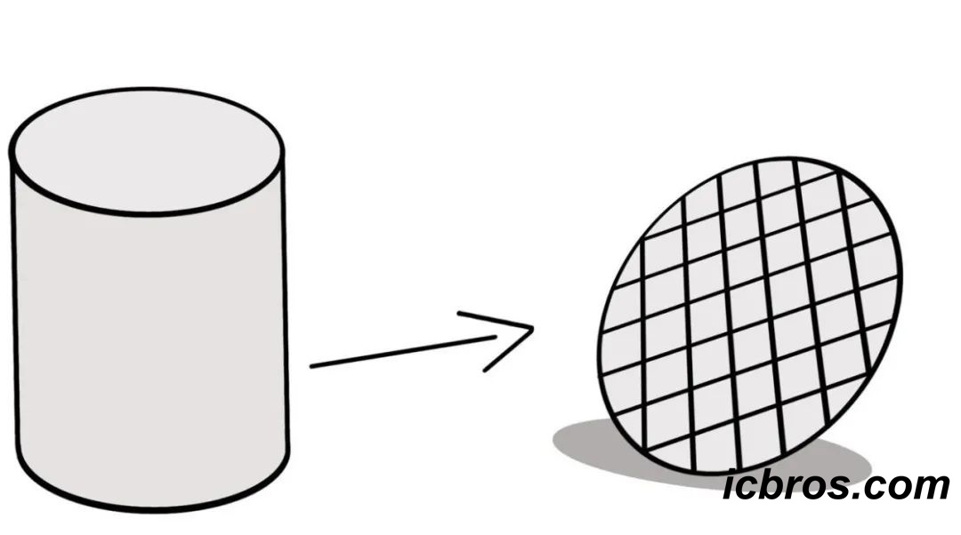
wafer fabrication 
Wafer lithography development and etching
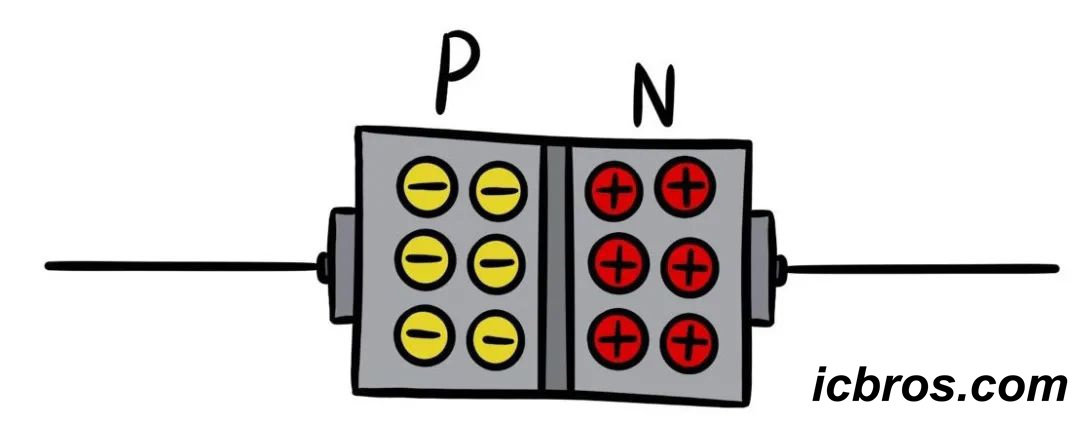
Impurities added
Packaging testing

research and development costs

The research and development cost of chips mainly includes expenses such as IP procurement, front-end design, validation, DFT design, back-end design, packaging design, and wafer back testing.
IP procurement
IP procurement is a crucial aspect in chip development that cannot be ignored.
The fee model is usually divided into one-time authorization, individual product authorization, or a combination of the two.
Wafer back testing
The chip back testing includes testing hardware, RA (Reliability Test) experiments, ATE (Automatic Test Equipment) machine usage, and R&D manpower investment.
other
The expenses for front-end design, verification, DFT design, back-end design, and packaging design are mainly based on the manpower investment of R&D personnel. In addition, they also include the cost of using EDA software, as well as the hardware cost of verification platforms such as FPGA and Zebu.
production cost
The production cost of chips mainly includes chips, wafers, CP (Chip Probe) testing, packaging, FT (Final Test), SLT (System Level Test), etc., with the majority concentrated in chips and wafers.
Chip cost
Streaming refers to making chips through a series of process steps like assembly lines. In the field of integrated circuit design, "streaming" refers to "pilot production".
Wafer cost
Calculate based on the number of shipped pieces per piece.

Wafer prices are also differentiated based on process nodes. TSMC's 12 inch wafer costs approximately $1500 to $2000 per 40nm chip, $4000 to $5000 per 16nm chip, $9300 per 7nm chip, $17000 per 5nm foundry, and $30000 per 3nm chip.


ICBROS TECHNOLOGY LIMITED is a worldwide professional electronic components distributor.

Web:https://www.icbros.com
Email:service@icbros.com
#DAC #pcbuild #icbros #analogelectronics #semimodular #preamplifier #elettronica #supercon #pcbengineer #diyelectronics #eletricistas #emeddedsystems #hobielektronik #electricalprojects #components #makers #engineering #irremote #studentproject #pic24 #eletronica #drscientist #universalrobots #circuitplayground #powersupply #arduinocompatible

Related News

With a maximum throughput of 46.4 Gbps, Kioxia has started mass production of UFS 4.0 flash chips

With a maximum throughput of 46.4 Gbps, Kioxia has started m

Our hot chip models today 3

Our hot chip models today 3

Meta launched the AI language model LLaMA, a large language model with 65 billion parameters

Meta launched the AI language model LLaMA, a large language

India's domestic chip plan has been hit again, with news saying that the $3 billion project for Gaota Semiconductor has been indefinitely shelved

India's domestic chip plan has been hit again, with news say

Discussion on the integrated solution of

Discussion on the integrated solution of "semiconductor" pho

No need to change the band frequently, Apple is studying the variable color Apple Watch strap

No need to change the band frequently, Apple is studying the

Product Categories

  • Factory Overview
  • SMT Assembly
  • DIP Assembly
  • Testing Equipment
  • Conformal Coating
  • Final Assembly
  • Factory Overview
  • SMT Assembly
  • DIP Assembly
  • Testing Equipment
  • Conformal Coating
  • Final Assembly

Links

内页左侧广告1

LatestPost

Feedback

Contact Us

+852 44058386

+852 44058386

cici@vip.icbros.com

live:.cid.497a4afb2eba768b

5/F, Ming Sang Industrial Building, No 21 Hing Yip Street,Kwun Tong, Kowloon, Hong Kong, 15th Floor, World Trade Building, Futian District, Shenzhen, China

MOBILE WEBSITE

Copyright © 2013-2026 All Rights Reserved.

  • Skype.
  • E-mail
  • Whatsapp
  • Inquiry
Inquiry Us Now !
Inquiry Us Now !